مقالة علمية بعنوان (Pulsed laser deposition)
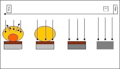
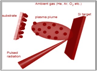
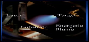
Pulsed laser deposition method is one of the simple methods because it does not require equipment of complex nature to prepare thin films of conductive and semiconductor materials as well as insulators , This method works on the formation of nanoparticles with a size of between (100-10 nm). And that this process includes three basic stages, which are heating, thermal diffusion and fusion at the point of impact, after which evaporation takes place and the plasma flames away from the surface of the target Then the fragmented materials are collected on slides of glass or silicon, and this leads to a condensation process of the material on the surface of the base, which leads to the formation of a thin film. The specifications of the thin films that are formed depend on the deposition conditions such as (the energy of the laser pulse used, the substrate temperature, the number of pulses, the wavelength of the laser and the type of gas used in the vacuum chamber) And that the target absorption of the laser beam is very important in order for the laser scraping process to occur, and that this process is the main source of energy inside the reacting material, and because the laser pulse occurs in a very short period, it is the reason for the occurrence of the three processes in a very short time, which leads to the occurrence of a number of stresses inside the material. <br /><br />بواسطة : م.م. حوراء عبد الكريم عليوي