
تكنولوجيا الافلام الرقيقة
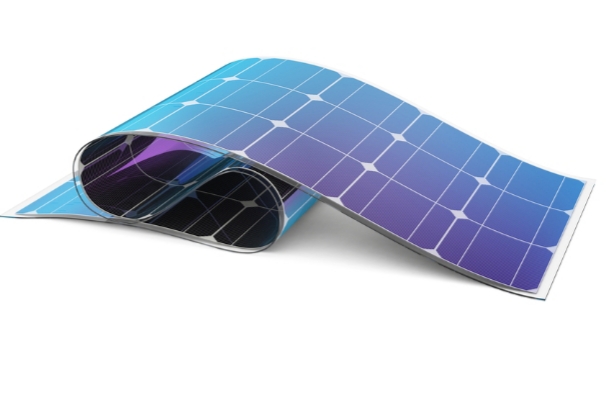
Thin Film Technology <br />Assist.Lec.Qunoot Mohammed Hadi <br />A thin film is a layer of material ranging from fractions of a nanometer (monolayer) to several micrometers in thickness. The controlled synthesis of materials as thin films (a process referred to as deposition) is a fundamental step in many applications. A familiar example is the household mirror, which typically has a thin metal coating on the back of a sheet of glass to form a reflective interface. The process of silvering was once commonly used to produce mirrors, while more recently the metal layer is deposited using techniques such as sputtering. Advances in thin film deposition techniques during the 20th century have enabled a wide range of technological breakthroughs in areas such as magnetic recording media, electronic semiconductor devices, LEDs, optical coatings (such as antireflective coatings), hard coatings on cutting tools, and for both energy generation (e.g. thin-film solar cells) and storage (thin-film batteries). It is also being applied to pharmaceuticals, via thinfilm drug delivery. A stack of thin films is called a multilayer. In addition to their applied interest, thin films play an important role in the development and study of materials with new and unique properties. Examples include multiferroic materials, and superlattices that allow the study of quantum phenomena. Physical deposition uses mechanical, electromechanical or thermodynamic means to produce a thin film of solid. An everyday example is the formation of frost. Since most engineering materials are held together by relatively high energies, and chemical reactions are not used to store these energies, commercial physical deposition systems tend to require a low-pressure vapor environment to function properly; most can be classified as physical vapor deposition (PVD). The material to be deposited is placed in an energetic, entropic environment, so that particles of material escape its surface. Facing this source is a cooler surface which draws energy from these particles as they arrive, allowing them to form a solid layer. The whole system is kept in a vacuum deposition chamber, to allow the particles to travel as freely as possible. Since particles tend to follow a straight path, films deposited by physical means are commonly directional, rather than conformal. Examples of physical deposition include: A thermal evaporator that uses an electric resistance heater to melt the material and raise its vapor pressure to a useful range. This is done in a high vacuum, both to allow the vapor to reach the substrate without reacting with or scattering against other gas-phase atoms in the chamber, and reduce the incorporation of impurities from the residual gas in the vacuum chamber. Obviously, only materials with a much higher vapor pressure than the heating element can be deposited without contamination of the film. Molecular beam epitaxy is a particularly sophisticated form of thermal evaporation. An electron beam evaporator fires a high-energy beam from an electron gun to boil a small spot of material; since the heating is not uniform, lower vapor pressure materials can be deposited. The beam is usually bent through an angle of 270° in order to ensure that the gun filament is not directly exposed to the evaporant flux. Typical deposition rates for electron beam evaporation range from 1 to 10 nanometres per second. In molecular beam epitaxy (MBE), slow streams of an element can be directed at the substrate, so that material deposits one atomic layer at a time. Compounds such as gallium arsenide are usually deposited by repeatedly applying a layer of one element (i.e., gallium), then a layer of the other (i.e., arsenic), so that the process is chemical, as well as physical; this is known also as atomic layer deposition. If the precursors in use are organic, then the technique is called molecular layer deposition. The beam of material can be generated by either physical means (that is, by a furnace) or by a chemical reaction (chemical beam epitaxy). Sputtering relies on a plasma (usually a noble gas, such as argon) to knock material from a "target" a few atoms at a time. The target can be kept at a relatively low temperature, since the process is not one of evaporation, making this one of the most flexible deposition techniques. It is especially useful for compounds or mixtures, where different components would otherwise tend to evaporate at different rates. Note, sputtering's step coverage is more or less conformal. It is also widely used in optical media. The manufacturing of all formats of CD, DVD, and BD are done with the help of this technique. It is a fast technique and also it provides a good thickness control. Presently, nitrogen and oxygen gases are also being used in sputtering. Pulsed laser deposition systems work by an ablation process. Pulses of focused laser light vaporize the surface of the target material and convert it to plasma; this plasma usually reverts to a gas before it reaches the substrate. Cathodic arc deposition (arc-PVD) which is a kind of ion beam deposition where an electrical arc is created that literally blasts ions from the cathode. The arc has an extremely high power density resulting in a high level of ionization (30–100%), multiply charged ions, neutral particles, clusters and macro-particles (droplets). If a reactive gas is introduced during the evaporation process, dissociation, ionization and excitation can occur during interaction with the ion flux and a compound film will be deposited. Electrohydrodynamic deposition (electrospray deposition) is a relatively new process of thin-film deposition. The liquid to be deposited, either in the form of nanoparticle solution or simply a solution, is fed to a small capillary nozzle (usually metallic) which is connected to a high voltage. The substrate on which the film has to be deposited is connected to ground. Through the influence of electric field, the liquid coming out of the nozzle takes a conical shape (Taylor cone) and at the apex of the cone a thin jet emanates which disintegrates into very fine and small positively charged droplets under the influence of Rayleigh charge limit. The droplets keep getting smaller and smaller and ultimately get deposited on the substrate as a uniform thin layer. Growth modes:Frank-van der Merwe growth ("layer-by-layer"). In this growth mode the adsorbate-surface and adsorbate-adsorbate interactions are balanced. This type of growth requires lattice matching, and hence considered an "ideal" growth mechanism. Stranski–Krastanov growth ("joint islands" or "layer-plus-island"). In this growth mode the adsorbate-surface interactions are stronger than adsorbate-adsorbate interactions. Volmer-Weber ("isolated islands"). In this growth mode the adsorbate-adsorbate interactions are stronger than adsorbate-surface interactions, hence "islands" are formed right away. <br />